In the digital age, we are surrounded by invisible cities of thought. Every click, every streamed video, and every complex calculation in the servers that power our world relies on a fundamental component: Random Access Memory (RAM). This dynamic, lightning-fast workspace for your computer’s processor is a masterpiece of modern engineering. Its creation is not merely manufacturing; it is an exercise in atomic-scale precision, conducted in some of the most controlled environments on Earth. The journey from a pile of sand to a sleek memory module is a saga of human ingenuity.
Our story begins not with silicon, but with extreme purification. The raw material is common quartzite sand, rich in silicon dioxide. This sand is melted in massive arc furnaces at temperatures exceeding 2,000°C, and through a series of chemical reactions, is transformed into metallurgical-grade silicon. Yet this is still far too impure for electronics. The silicon is then converted into a liquid trichlorosilane gas, which is distilled to razor-sharp purity before being deposited in a Chemical Vapor Deposition (CVD) reactor. Here, around a thin, rotating seed crystal of pure silicon, the magic happens. The gas decomposes, and pure silicon atoms slowly, atom by atom, build upon the seed, growing into a flawless, cylindrical single crystal ingot. This process, called the Siemens process, can take days, resulting in a shimmering metallic pillar up to two meters long.
This ingot is then ground to a perfect diameter and, using a diamond saw thinner than a human hair, sliced into wafers—discs as thin as a credit card but perfectly flat and polished to a mirror finish. A typical wafer today is 300mm (12 inches) in diameter. These wafers are the blank canvases upon which the memory will be painted. Their surface must be atomically smooth, as any imperfection measured in nanometers could ruin billions of transistors.
The actual fabrication of the memory cells happens in a semiconductor fab, a facility so clean it makes a hospital operating room look dusty. Air is filtered to remove particles larger than a few nanometers, and technicians, or “fab rats,” are clad head-to-toe in bunny suits to prevent human contamination. Here, the wafer undergoes a repetitive, intricate ballet of patterning, doping, and layering—a process that can involve over 500 steps.
The heart of RAM, particularly the prevalent DRAM (Dynamic RAM), is the memory cell: one transistor and one capacitor. The capacitor stores an electrical charge (a ‘1’ or ‘0’), and the transistor acts as a gatekeeper, controlling access to it. Packing billions of these into a thumbnail-sized chip requires near-impossible geometry. The defining technology is photolithography. A liquid light-sensitive resin called photoresist is spun onto the wafer. Then, using a machine called a stepper or scanner—the most expensive and complex tool in the fab—a pattern of the circuit is projected onto the wafer using extreme ultraviolet (EUV) light with a wavelength of just 13.5 nanometers. This light, generated by firing lasers at microscopic tin droplets, is the only way to etch features now just a few dozen atoms wide. The exposed resist hardens, and the unexposed areas are washed away, creating a stencil for the next step.
Through this stencil, the wafer is bombarded with ions (doping) to alter the silicon’s electrical properties, or layers of insulators (like silicon nitride) and conductors (like copper or tungsten) are deposited. The capacitor, which must have a large surface area to hold charge but occupy a minuscule footprint, is built vertically—etching deep, cylindrical holes into the silicon and lining them with conductive materials, creating a microscopic tower. This 3D structuring is key to modern density. This cycle of lithography, etching, doping, and deposition repeats dozens of times, building up the complex, multi-layered cityscape of the memory chip.
Once the wafer is complete, covered in a grid of identical rectangular patterns (the “dies”), it undergoes rigorous electronic testing. Probes finer than a human hair touch down on the tiny contact pads of each die, sending and receiving test signals. Faulty dies are instantly mapped and marked with an ink dot. Given the astronomical complexity, even on a mature production line, perfection is elusive; yield management is a constant battle of physics and statistics.
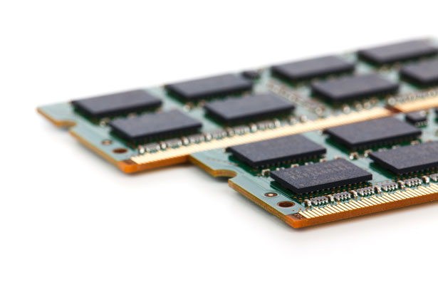
The good dies are then carefully sliced from the wafer by a diamond saw or, more recently, by a process called stealth dicing using lasers. Each functional die, now called a chip, is ready for packaging. It is placed onto a substrate—a small green printed circuit board—and connected using gold or copper wires so fine they are almost invisible, or via the more advanced flip-chip method where tiny solder bumps on the chip’s face are directly bonded to the substrate. This package protects the delicate silicon and provides the connective pins or balls that will link it to the outside world.
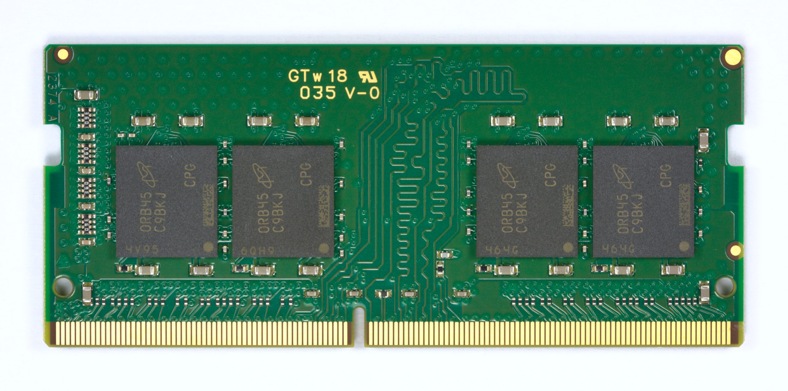
For a RAM module like a DIMM (Dual In-line Memory Module), the final act is assembly. Multiple packaged chips, typically 8 or 16, are robotically placed onto a longer PCB. They are soldered into place, and the module undergoes another round of intense testing for speed, timing, and stability at varying voltages and temperatures. Only modules that pass muster are fitted with their distinctive aluminum heat spreaders (often purely for aesthetics in consumer modules) and slotted into anti-static bags, ready for their journey into a server farm, gaming rig, or smartphone.
The manufacture of RAM is a testament to a globalized, hyper-specialized industry. It represents a pinnacle of physics, chemistry, materials science, and software, with a single fab costing upwards of $20 billion. It is a process conducted at the scale of atoms, where quantum effects begin to whisper challenges for the next generation. As we demand more memory, faster, and with lower power, the industry answers by building upwards, into intricate 3D structures, and onwards, pushing the limits of light itself. The next time your computer instantly loads an application, remember the invisible, atomic metropolis working tirelessly behind the scenes—a city built not of steel and concrete, but of purified sand, sculpted by light.