In the palm of your hand, inside your laptop, or at the heart of a data center server, lies one of humanity’s most profound creations: the Central Processing Unit (CPU). This tiny silicon chip, often no larger than a thumbnail, can contain tens of billions of transistors, each acting as a minuscule electronic switch. The process of manufacturing this microscopic metropolis is a breathtaking ballet of physics, chemistry, and precision engineering, often described as the most complex manufacturing feat ever mastered. Let’s embark on the odyssey of how sand is transformed into the brain of a computer.
Stage 1: From Beach Sand to Perfect Crystal – Creating the Silicon Wafer
Our journey begins not in a sterile factory, but on a beach. Silicon, the second most abundant element in the Earth’s crust, is derived from silica sand. This sand is purified in a multi-step process to create Electronic Grade Silicon (EGS), an ingot of hyper-pure, polycrystalline silicon that is 99.9999999% pure (“nine nines” pure).
Next comes the Czochralski Process. A small seed crystal of silicon is dipped into a molten vat of EGS and slowly rotated and pulled upward. As it ascends, silicon from the melt solidifies onto the seed, perfectly aligning with its crystalline structure. The result is a flawless, cylindrical single-crystal ingot, typically 300mm (12 inches) in diameter and up to 2 meters long—a gigantic silicon pencil.
This ingot is then ground to a perfect diameter, its orientation flats are etched, and it is sliced into wafers using an ultra-thin diamond saw. These raw wafers are polished to a mirror-smooth, flawless finish, ready to become the canvas for hundreds of CPU dies.
Stage 2: The Heart of the Process – Photolithography and Patterning
Now the true magic begins. The creation of transistors and circuits on the wafer is achieved through a cyclical process called photolithography, repeated dozens of times to build up the CPU’s layered 3D structure.
- Oxidation and Coating: The wafer is first heated, creating a thin insulating layer of silicon dioxide on its surface. Then, a light-sensitive liquid called photoresist is evenly spun onto the wafer.
- Exposure – The Art of Shrinking: This is the most critical and challenging step. A photomask—a glass plate containing the pattern for one layer of the circuit (like a stencil)—is placed over the wafer. In modern EUV (Extreme Ultraviolet) lithography machines, which cost upwards of $150 million, light of an incredibly short wavelength (13.5 nanometers) is shined through the mask, projecting its pattern onto the photoresist. The goal is to print features that are just a few nanometers apart—smaller than a virus. This step requires astonishing precision, with wafers and lenses stabilized to counteract even the slightest vibration.
- Development and Etching: The exposed photoresist is chemically “developed,” washing away the parts that were hit by light (in a positive resist process). What remains is a protective layer in the desired pattern. The wafer is then subjected to etching, where plasma gases or chemicals attack the unprotected areas, carving the circuit pattern into the silicon dioxide or silicon layer beneath.
- Doping and Deposition: With the pattern etched, specific regions of the silicon are bombarded with ions (doping) to alter their electrical properties, creating the essential “n-type” and “p-type” semiconductors that form transistors. Subsequent steps use Chemical Vapor Deposition (CVD) or Physical Vapor Deposition (PVD) to blanket the entire wafer with new ultra-thin layers of insulating or conductive materials (like copper or tungsten).
- Planarization (CMP): After deposition, the surface is uneven. Chemical Mechanical Planarization (CMP), a high-tech polishing process, grinds the surface down to a perfectly flat plane, ready for the next lithography cycle.
This sequence—coat, expose, develop, etch, dope, deposit, polish—is repeated 30 to 50 times for a modern CPU. Each cycle defines a new layer, from the deepest transistor wells to the highest-level copper interconnects (the “wires” that link transistors).
Stage 3: Testing, Slicing, and Packaging – From Wafer to Chip
Once the wafer is fully patterned, it undergoes a first round of rigorous testing. Ultra-fine probes contact the tiny pads on each individual CPU die to check for basic functionality. A map of the wafer is created, marking which dies are good and which are faulty.
The wafer is then placed on a sticky film and cut into individual dies using a diamond-tipped saw in a process called dicing. The functional dies are picked from this film, while the faulty ones are discarded.
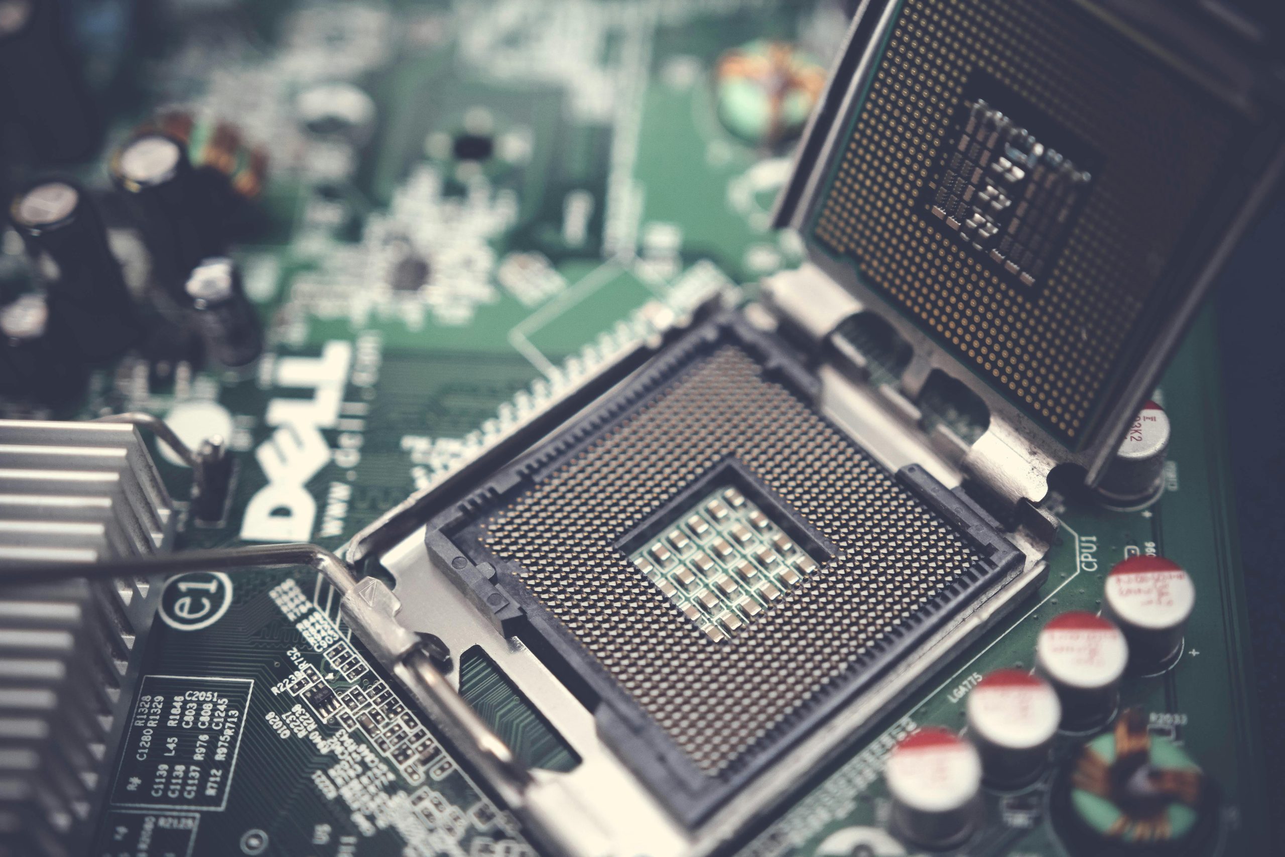
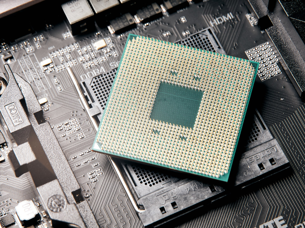
A naked silicon die is incredibly fragile. Packaging is the process of giving it protection and a means to communicate with the outside world. The die is placed onto a substrate (a small green circuit board), and gold or copper wires finer than a human hair, or more commonly now, microscopic solder bumps in a “flip-chip” process, connect its pads to the substrate’s pins. A heat-spreading Integrated Heat Spreader (IHS)—the shiny metal cap you see on a CPU—is then glued on top. This cap protects the die and provides a surface for a cooler to be mounted.
Stage 4: The Final Exam – Bin Sorting and Validation
The packaged CPU is not yet ready for sale. It undergoes its final, most comprehensive testing. It is inserted into a high-speed tester that runs it at various frequencies and voltages, pushing it to its limits. This process determines its final performance characteristics.
Not all CPUs come out identical due to microscopic variations in the manufacturing process. Testing reveals which chips can run stably at higher speeds with lower power. This is where bin sorting occurs: a chip that meets the specs for a top-tier Core i9 model will be labeled and priced as such, while one that performs at a lower stable frequency might become a Core i5. This allows manufacturers to maximize yield from every wafer.
Only after passing this gauntlet is a CPU branded, placed in its protective packaging, and shipped to become the engine inside a device, ready to execute billions of calculations per second.
A Symphony of Precision
The CPU manufacturing process is a testament to human ingenuity. It is conducted in some of the cleanest environments on Earth—Class 1 cleanrooms where a single dust particle could be a boulder-sized defect. It leverages quantum mechanical phenomena to manipulate materials a few atoms thick. From a mound of sand to a chip that can simulate galaxies, compose music, and connect humanity, the creation of a CPU is not just manufacturing; it is the meticulous construction of a microscopic universe, one atom at a time. It remains, quite simply, the pinnacle of modern industrial art.