In an era defined by artificial intelligence, cinematic gaming, and scientific simulation, the Graphics Processing Unit (GPU) stands as a cornerstone of modern computing. These intricate silicon brains, capable of performing trillions of calculations per second, begin their life not in a sterile lab, but as one of the planet’s most common materials: sand. The transformation of raw quartz into a finished GPU is a marathon of precision engineering, fundamental physics, and global collaboration, representing one of humanity’s most advanced manufacturing feats.
Stage 1: The Birth of Pure Silicon – From Sand to Ingot
The journey begins with silica sand, particularly quartz, which has a high percentage of silicon dioxide (SiO₂). This sand is first melted in a furnace at temperatures exceeding 2,000°C and reacted with carbon to remove oxygen, resulting in metallurgical-grade silicon (about 99% pure). For the ultra-purity required by semiconductors, this silicon undergoes further refinement via the Siemens Process. Here, silicon is converted into a gas (trichlorosilane) and then deposited onto a thin rod of pure silicon in a high-temperature chamber. This builds up a massive, cylindrical crystal of electronic-grade polycrystalline silicon, which is 99.9999999% pure—often called “nine nines” pure.
This ultra-pure silicon is then melted again in a crucible under an inert argon atmosphere. A tiny seed crystal, aligned to a specific atomic orientation, is dipped into the melt and slowly pulled upwards while rotating. The silicon atoms from the melt align with the seed’s crystal structure, growing a flawless, single-crystal cylinder called an ingot. This process, known as the Czochralski method, produces ingots up to 300mm (12 inches) in diameter and over 1.5 meters long, weighing several hundred kilograms.
Stage 2: Engineering the Silicon Canvas – Wafer Production
The giant ingot is ground to a perfect diameter and its conductivity is tested. Using a diamond-tipped saw, it is then sliced into discs as thin as a millimeter, called wafers. These wafers are polished to a flawless, mirror-smooth finish, eliminating any microscopic imperfections from the slicing process. This pristine silicon wafer becomes the foundational canvas upon which hundreds of GPU chips will be built.
Before any circuit is created, the wafer undergoes an oxidation process, growing a thin, uniform layer of silicon dioxide (SiO₂) on its surface. This layer acts as an excellent electrical insulator and will serve as the base for the first critical step: photolithography.
Stage 3: Photolithography – Printing the Blueprint
This is the heart of GPU fabrication, where the complex circuit design is “printed” onto the wafer. It is a repetitive, cyclical process (often taking over 3 months and hundreds of steps) that builds the GPU layer by layer.
- Coating: The wafer is coated with a light-sensitive chemical called photoresist.
- Exposure: The wafer is placed in a photolithography machine (a “stepper” or “scanner”), one of the most expensive and precise tools on Earth. Using ultraviolet light, the machine projects the circuit pattern for one layer through a photomask (a master stencil of the chip design) onto the wafer. The wavelength of this light is critical; extreme ultraviolet (EUV) lithography, using light just 13.5nm in wavelength, is the latest breakthrough, allowing for impossibly small features.
- Development: The exposed photoresist is chemically washed away, leaving a precise pattern on the wafer surface that matches the mask.
Stage 4: Etching and Deposition – Sculpting the Nanoscape
With the photoresist pattern as a guide, the wafer undergoes etching. Unprotected areas of the silicon dioxide are etched away using potent gases or plasmas in a vacuum chamber, carving trenches and channels into the wafer. The remaining photoresist is then stripped.
Next, various materials are deposited. Through chemical or physical vapor deposition, thin films of insulators (like new SiO₂) or conductors (like copper or polysilicon) are layered over the entire wafer, filling the etched trenches. Excess material is then polished away using Chemical Mechanical Planarization (CMP), leaving a flat surface for the next layer.
This cycle—deposit, coat, expose, develop, etch, polish—is repeated dozens of times. Each layer connects to the ones below and above via tiny vertical tunnels called “vias,” eventually building up the three-dimensional cityscape of transistors, capacitors, and nanowires that form the GPU’s core.
Stage 5: Doping and Transistor Creation
The function of a semiconductor comes from its ability to precisely control electrical flow. This is achieved through doping—the intentional introduction of impurities like boron or phosphorus into specific regions of the silicon. By creating areas with an excess of electrons (n-type) or a deficit (p-type), the foundational building block of modern computing, the transistor, is formed. A modern GPU like the NVIDIA Ada Lovelace or AMD RDNA 3 architecture packs over 70 billion of these nanoscale switches into a chip the size of a thumbnail.
Stage 6: Testing, Slicing, and Packaging
Once fabrication is complete, the wafer holds hundreds of identical GPU dies. Each die is tested with microscopic probes. Faulty dies are marked for discard—the yield rate is a key metric for manufacturer efficiency.
A diamond saw then delicately cuts the wafer, separating the individual dies. The good dies are mounted onto a substrate—a small green circuit board that provides structural support and electrical connections. Using gold or copper wires finer than a human hair (or, in advanced packages, microscopic solder bumps in a “flip-chip” design), the die’s contact pads are connected to the substrate’s pins.
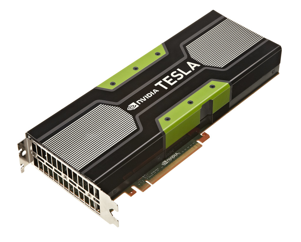
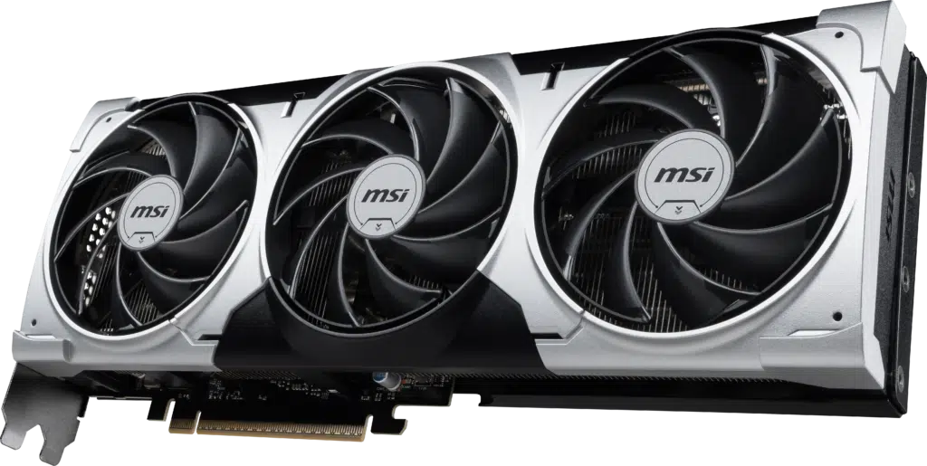
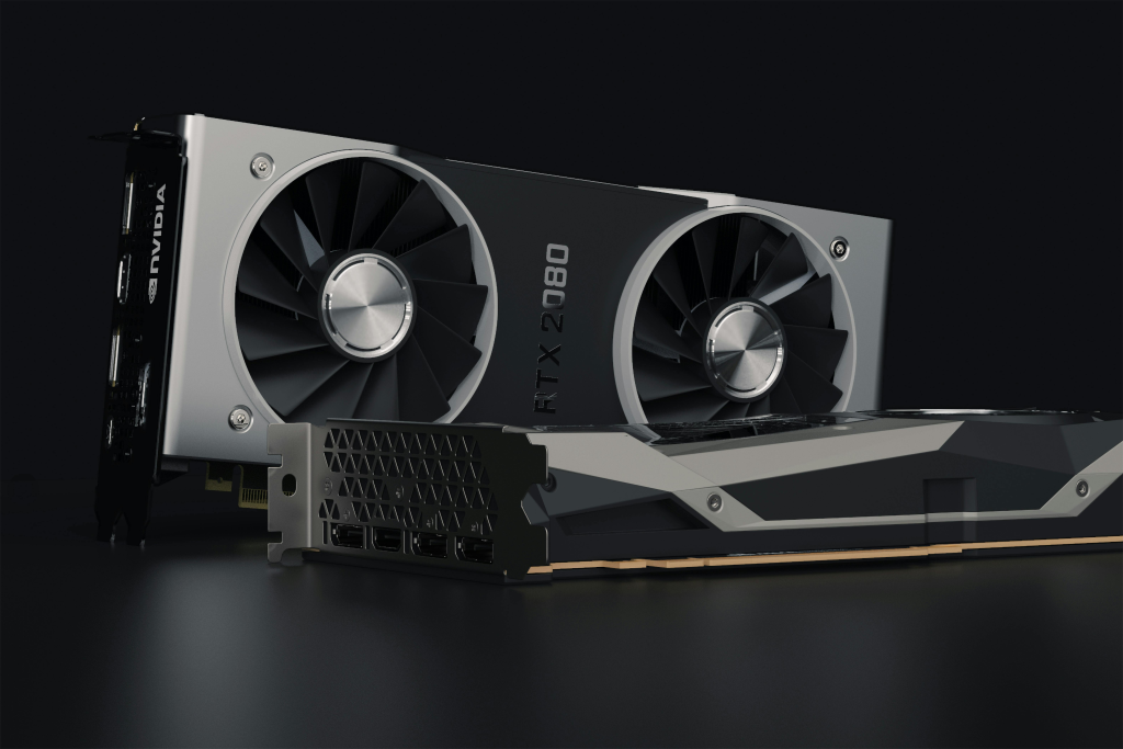
The die and its connections are then encased under a protective metal lid and heat spreader, often topped with the iconic brand logo. This packaging is crucial: it protects the fragile silicon, dissipates immense heat (a high-end GPU can output over 450 watts), and provides the physical interface (the pins or balls) to slot into a larger system.
Stage 7: The Final Product
The packaged GPU is placed onto its final Printed Circuit Board (PCB), surrounded by memory modules (GDDR6X/7), voltage regulation modules (VRMs), and cooling apparatus. After a final round of rigorous performance and stability testing, it is ready to be shipped, ultimately powering the experiences that define our digital world.
Conclusion: A Symphony of Scale and Precision
The manufacture of a GPU is less a simple assembly line and more a global symphony of physics, chemistry, and logistics. It involves thousands of steps, billions of dollars in facility investment (a single “fab” can cost $20 billion), and an unimaginable scale of miniaturization—transistors are now measured in angstroms, smaller than a strand of DNA. From humble sand to the engine of the AI revolution, the GPU’s journey is a testament to human ingenuity, a precise dance at the atomic scale that continues to push the boundaries of what is possible.