In the silicon heart of every computer, a relentless, invisible river of data flows between the processor and its memory. For decades, the architecture governing this flow—the dynamic random-access memory (DRAM) interface—was dominated by one technology: Double Data Rate (DDR) memory. From PCs to servers, DDR’s familiar sticks (DIMMs) have been the industry standard. However, as we push against the walls of Moore’s Law and demand ever-greater performance for artificial intelligence, high-performance computing, and advanced graphics, a new paradigm has emerged from the labs: High Bandwidth Memory (HBM). This isn’t just an incremental upgrade; it represents a fundamental rethinking of the relationship between memory and processor, setting the stage for a tectonic shift in computing architecture.
The Established Workhorse: DDR Memory
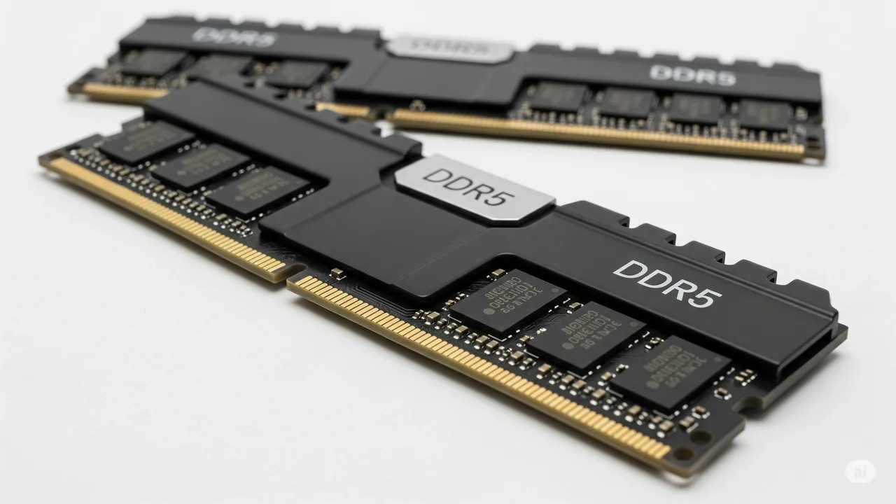
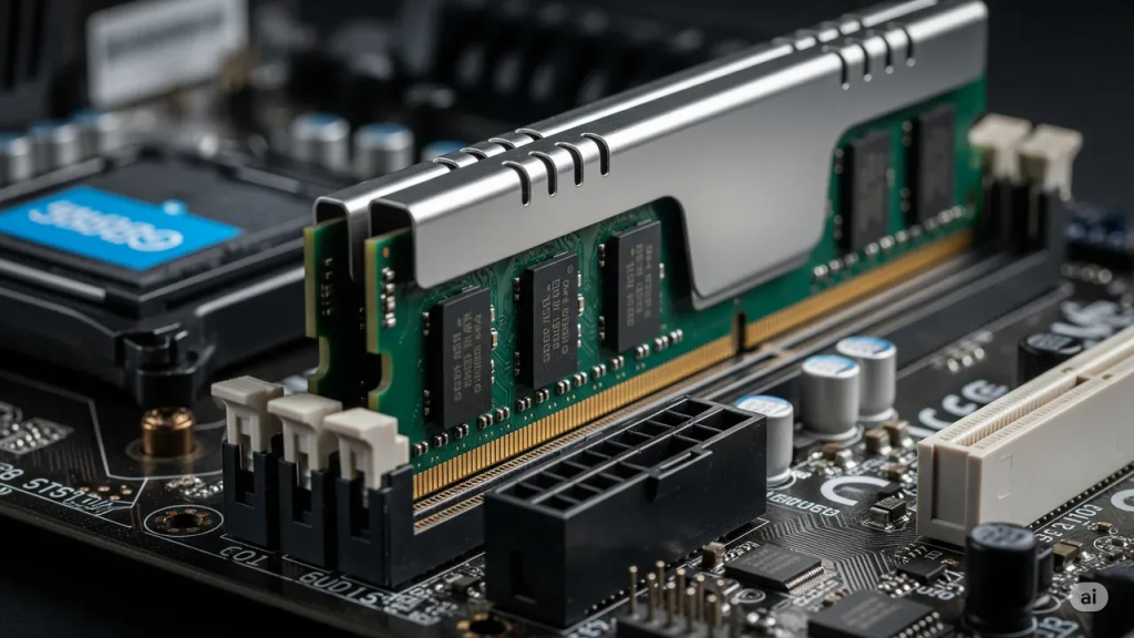
DDR memory, in its current fifth generation (DDR5), is the culmination of decades of evolution focused on speed and capacity within a cost-effective, modular framework. Its design principles are straightforward: memory chips are mounted on a printed circuit board (a DIMM), which plugs into a slot on the motherboard. Communication with the CPU happens across a 64-bit (or 128-bit in dual-channel) bus running at increasingly high clock speeds—DDR5 can operate at speeds beyond 6400 MT/s (Mega Transfers per second).
The key advantages of DDR are its modularity, cost-effectiveness, and high capacity. Users can easily upgrade system RAM by adding or swapping DIMMs, with capacities per module now reaching 128GB and beyond. This makes DDR ideal for general-purpose computing, where a balance of capacity, cost, and sufficient bandwidth is required for multitasking, running large applications, and data caching.
However, DDR faces intrinsic physical limitations. The data must travel from the DIMM slot, across motherboard traces (which can be several centimeters long), to the CPU’s memory controller. This journey introduces signal integrity challenges, latency, and power inefficiency at very high speeds. While the aggregate bandwidth increases with each generation (e.g., DDR5-6400 offers ~51.2 GB/s per channel), it does so by pushing clock rates higher, which increases power consumption and heat. The interface’s relatively narrow bus (64-bit) means it must run extremely fast to move large volumes of data, hitting a wall of diminishing returns.
The Disruptive Innovator: HBM Memory
High Bandwidth Memory, pioneered by companies like AMD and SK Hynix, takes a radically different approach. Instead of spreading out, HBM stacks up. Multiple DRAM dies (typically 4, 8, or even 12) are vertically stacked using through-silicon vias (TSVs)—microscopic vertical conduits that connect each layer. This 3D stack is then placed side-by-side with the processor (CPU or GPU) on the same interposer—a silicon substrate that acts as a super-high-density “middleman” connecting the two. This entire assembly is known as 2.5D packaging.
This architectural leap yields transformative benefits:
- Colossal Bandwidth: HBM’s genius is its ultra-wide bus. While DDR uses a 64-bit bus, HBM2e and HBM3 use a 1024-bit bus per stack. It’s the difference between a single-lane highway (running at blistering speeds) and a 16-lane superhighway (running at a moderate, efficient pace). This results in staggering bandwidth figures. A single HBM3 stack can deliver over 1 TB/s of bandwidth, dwarfing even quad-channel DDR5 systems.
- Extreme Energy Efficiency: Shorter data paths (on the order of millimeters instead of centimeters) and lower operating voltages and clock speeds translate to vastly superior bandwidth per watt. HBM can deliver data at a fraction of the energy cost of DDR, a critical factor in power-constrained environments like data centers.
- Radically Reduced Footprint: By going vertical, HBM occupies a tiny fraction of the physical space required for an equivalent amount of DDR capacity. This is essential for compact, performance-dense systems like accelerator cards.
The trade-offs, however, are significant. HBM is vastly more complex and expensive to manufacture, involving advanced packaging, testing, and stacking processes. Its capacity per stack is limited by the number of layers that can be reliably stacked (currently up to 24GB per HBM3E stack, with 36GB coming). Unlike DDR, it is not user-upgradeable; it is soldered onto the interposer as part of a cohesive subsystem, making it a permanent, fixed component of the processor package.

Clash of the Titans: Application-Driven Divergence
The choice between DDR and HBM is not about which is universally “better,” but about which is optimal for the workload.
DDR remains the king of general-purpose and capacity-centric computing.
- Client PCs & Servers: Where upgradability, large memory pools (512GB+), and cost-per-gigabyte are paramount.
- Enterprise Databases & Cloud Virtualization: Applications that benefit from massive in-memory datasets rather than raw memory throughput.
HBM is the undisputed champion of bandwidth-bound, performance-critical computing.
- AI & Machine Learning: Training massive neural networks involves constant, immense data shuffling between the GPU/TPU and memory. HBM’s bandwidth is the fuel for the AI revolution.
- High-Performance Computing (HPC): Scientific simulations in fields like computational fluid dynamics, climate modeling, and genomics are bottlenecked by memory bandwidth. HBM accelerates discovery.
- Premium Graphics & GPUs: High-end GPUs for professional visualization and gaming have been early and enduring adopters of HBM to feed their enormous parallel cores.
- Network Processing & Advanced Chipsets: The latest data center switches and dedicated ASICs integrate HBM to handle terabit-scale data flows.
The Future: Coexistence and Convergence
The landscape is not purely binary. We are entering an era of heterogeneous memory systems. Modern high-performance CPUs and accelerators increasingly feature both.
A flagship data center GPU might be equipped with HBM2e or HBM3 for its ultra-fast, local frame buffer, while the server it resides in uses DDR5 for the substantial system memory. This creates a tiered memory hierarchy: small, ultra-fast HBM cache close to the compute cores, backed by larger, slower, cheaper DDR main memory. Technologies like AMD’s Infinity Cache or NVIDIA’s Grace Hopper superchip architecture exemplify this sophisticated, multi-tiered approach.
Furthermore, the technologies are influencing each other. Innovations driven by HBM’s TSV and packaging challenges are trickling into mainstream memory. Meanwhile, the relentless demand for higher bandwidth is pushing DDR to evolve with techniques like on-DIMM buffering (as seen in DDR5) that borrow concepts from HBM’s playbook.
Conclusion
DDR and HBM represent two distinct philosophies in memory design. DDR is the scalable, versatile, and economical workhorse, built for capacity and flexibility. HBM is the specialized, high-throughput powerhouse, engineered for maximum bandwidth and efficiency in a compact form. As computing fragments into specialized workloads—from sprawling cloud instances to focused AI training clusters—the memory architecture is fragmenting to match. HBM is not a replacement for DDR; it is its complement at the apex of performance. Together, they form the tiered memory foundation upon which the next generation of computing—from personalized AI assistants to planet-scale climate models—will be built. The race for data is endless, and in the engines of innovation, both DDR and HBM will continue to play pivotal, if distinct, roles.